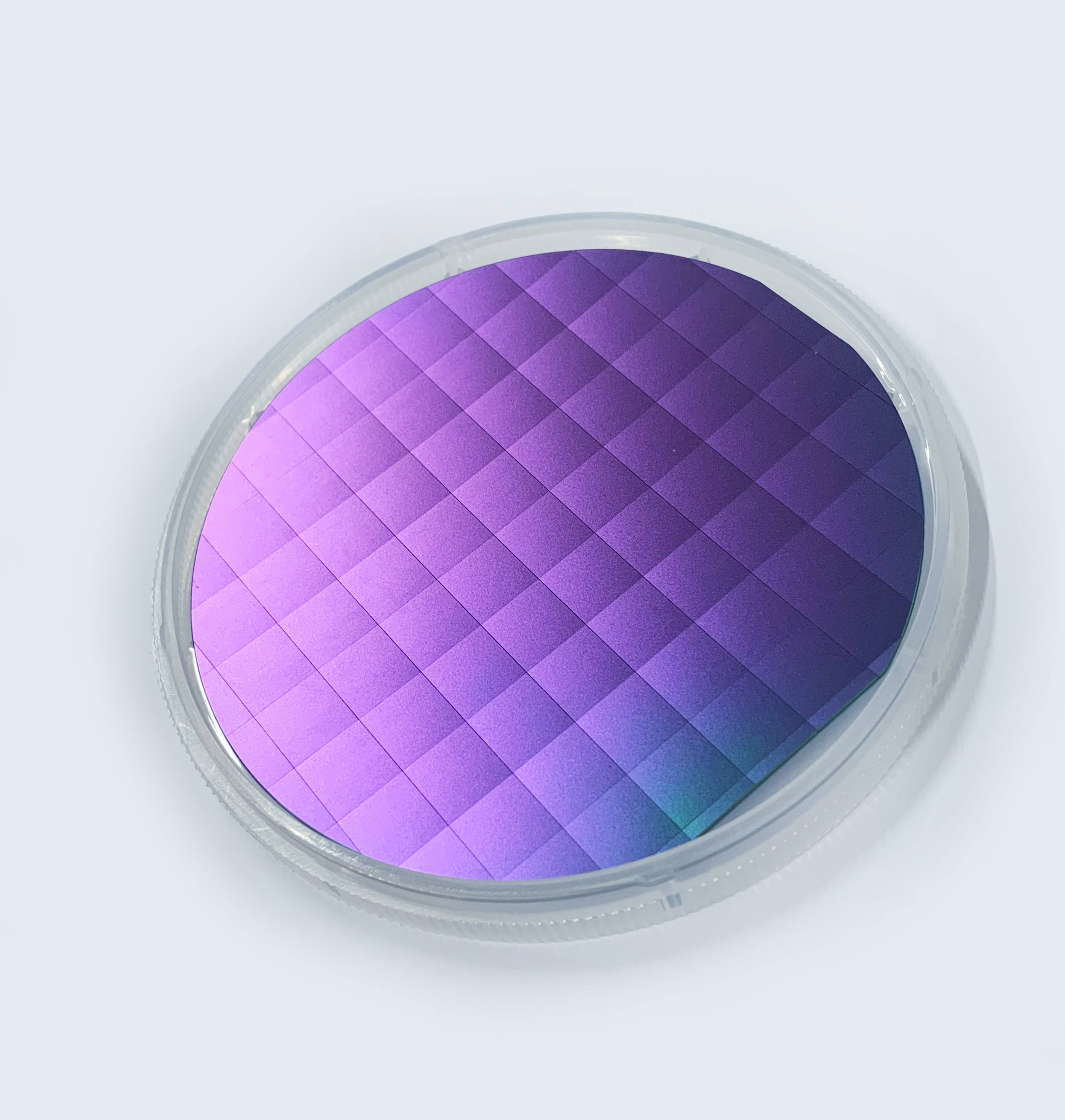
PI-KEM provides an extensive choice of wafers including glass, silicon, germanium, and other semiconductor materials. Alongside this we also offer a range of processing services for our silicon, sapphire, and single crystal wafers.
Coatings
Wafer coating is a versatile process that can be used to improve the performance, reliability, and manufacturability of wafers in a wide range of industries.
Wafers can be coated for a variety of reasons, including:
- Protection: Giving protection from environmental factors for example; Oxidation, contamination, and moisture. Important for wafers used in semiconductor manufacturing, where even a small defect can ruin a microchip.
- Improved performance: Can provide electrical insulation, reduction of friction, or enhanced optical properties.
- Ease of processing: Provide a smooth surface for deposition of other materials or make the wafer more resistant to etching
Specific examples of why wafers are coated in different industries include:
- Semiconductor manufacturing: Used on silicon wafers to protect them from oxidation and contamination, and to provide electrical insulation. These coatings are also used as etch stop layers and as diffusion barriers.
- Solar cell manufacturing: Coated with anti-reflective coatings to improve their efficiency.
- Display manufacturing: Coated with metal coatings to provide electrical conductivity and to enhance optical properties.
PI-KEM can offer a variety of coatings which, dependent on coating type and application methods, can be applied in a range of thicknesses.
Laser Marking
Allowing tight quality control and traceability as each wafer has a unique identification number. Essential for batch monitoring for research, compliance with industry regulations and ongoing quality management.
Surface Finishes
PI-KEM can offer a variety of surface finishes to support research and production requirements
Polishing
Many applications, including semiconductor, sensor, and micro-electronic device manufacture, require wafers to have exact specifications, with tight tolerances, for flatness and thickness to ensure they work reliably and perform well. By polishing the wafers, these requirements can be achieved. Wafer polishing uses an abrasive slurry and specialist equipment to remove a thin layer from the surface of the wafer.
Polishing can be single sided (SSP) or double sided (DSP) and involves removing up to 10 microns from the wafer surface.
- Reduces thickness
- Reduces stress points caused by flaws developed during boule growth or wafer preparation so decreasing the chance of breakages
- Prevents warping, as strength and flexibility are increased.
- Produces a more enhanced wafer with a super smooth, uniform crystal surface for epitaxial thin film growth
- Prepares them for future processing. By reducing the number of defective devices, a higher yield can be achieved
As cut/sawn
These wafers are sliced from the raw silicon ingot before any other process is carried out. Their surfaces are rough and non-reflective. As-cut wafers can be used for basic research that does not require a highly finished surface or bought by manufacturers to process to their own specifications.
PI-KEM can offer up to 6” or 150mm diameter as cut/ sawn wafers.
Lapped
Lapping allows the production of wafers with a flat, smooth surface and tight tolerances of thickness, parallelism, flatness, or finish. By treating the wafer surface with a slurry and moving it over a lapping pad it gains a flat, matte, dull grey surface. These wafers can be used as is or be further processed with polishing.
Etched
Etched wafers are commonly used as the base for microelectronic devices. Etching can be carried out by wet or dry etching, both result in the removal of unwanted contaminants from the surface of the wafer.
PI-KEM can supply etched wafers to customers individual specifications. We also supply the Cheersonic coaters which enable customers to deposit their own photoresist and other coatings. Click here find out more about the Cheersonic equipment, or watch the video here.
Dicing Service
Individual wafers are cut into small chips or dies for customers own processing needs, including lithography, deposition, and etching.
Wafers are diced to customers specifications.
Options:
- Coating
- Dicing
- Etching
- Polishing
- Laser marking
- As cut or lapped
Materials:
- Silicon
- Glass
- Sapphire
- Germanium
- InPh
If the material you require is not listed, please contact our Business Development Team for support.
Service Overview Tables
Coatings
Surface
Dicing services


